LTC4350
4350fb
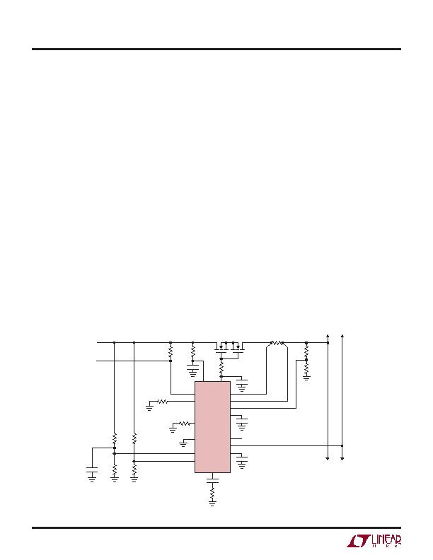
Figure 5. 5V Load Share (20A per Module)
When the power supply is disconnected, the UV pin will
drop below 1.220V if the supply is loaded. The LTC4350
then discharges the gate of the power FET isolating the
load from the power supply.
DESIGN EXAMPLE
Load Share Components
This section demonstrates the calculations involved in
selecting the component values. The design example in
Figure 5 is a 5V output. This design can be extended to
each of the parallel sections.
The first step is to determine the final output voltage and
the amount of adjustment on the output voltage. The power
supply voltage before the load sharing needs to be lower
than the final output voltage. If the load is expecting to see
a 5V output, then all of the shared power supplies need
to be trimmed to 4.90V or lower. This allows 2% variation
in component and reference tolerances so that the output
always starts below 5V .
Now that the output voltage is preset below the desired
output, the LTC4350 will be responsible for increasing the
output utilizing the SENSE
+
input to the power supply. If
a SENSE
+
line is not available, then the feedback divider
at the modules error amplifier can be used. The next step
is to determine the maximum positive adjustment needed
for each power supply. This adjustment includes any I " R
drops across sense resistors, power FETs, wiring and
connectors in the supply path between the power supply
and the load. For example, if the maximum current is 10A
and the parasitic resistance between the power supply and
load is 0.01? then the positive adjustment range for I " R
drops is 0.1V . Since the starting voltage is 4.9V ?.1V ,
then the lowest starting voltage can be 4.8V . This voltage
is 0.2V below the target. The total adjustment range that
the LTC4350 will need for this example is 0.1V + 0.2V =
0.3V . Note that the lowest starting voltage should not be
lower than 300mV below the target voltage.
The I " R drops should be designed to be low to elimi-
nate the need for additional bulk capacitance at the load.
In most cases the bulk capacitance exists at the power
supply output before the I " R drops. If a 0.002?sense
resistor is used and the FET resistance is below 0.003?
then a total 0.005?series resistance is acceptable for
loads to 20A. Obviously, the FB pin compensates for the
DC output impedance, but the AC output impedance is the
I " R drops plus the ESR of the capacitors.
4
3
2
1
R
GAIN
86.6k
R
SET
100
GAIN
R
SET
I
OUT
R
+
R
FB
TIMER
C
T
0.1礔
STATUS
STATUS
4350 F05
SB
COMP1
V
CC
GATE
GND
COMP2
LTC4350
UV
OV
C
P1
1000pF
C
P2
1礔
R
P1
150
43.2k
274k
12.1k
121k
C
G
0.1礔
0.1礔
OUT
+
ENSE
+
4.9V NOMINAL, 5.3V MAXIMUM
R
G
100
R
SENSE
0.002
37.4k
5V
BUS
12.1k
R
OUT
30
51
4 SUD50N03-07
(0.007 EACH)
SHARE
BUS
C
UV
0.1礔
applicaTions inForMaTion
发布紧急采购,3分钟左右您将得到回复。
相关PDF资料
MAX1299CEAE+
IC TEMP SENS W/ADC 16-SSOP
MAX14544ETA+T
IC ACCY SWITCH OVP PROTECT 8TDFN
MAX1617AMEE+T
IC REMOTE/LOCAL TEMP SNSR 16QSOP
MAX1617MEE+T
IC REMOTE/LOCAL TEMP SNSR 16QSOP
MAX1619MEE+
IC TEMP SENSOR W/ALARM 16-QSOP
MAX1765EUE+
IC REG DL BST/LINEAR 16TSSOP
MAX1989MUE+
IC TEMP SENSOR REMOTE 16TSSOP
MAX31723MUA+
IC THERMOMETER/STAT SPI-3W 8UMAX
相关代理商/技术参数
LTC4350IGN#TR
功能描述:IC CNTRLR HOTSWAP LOADSHAR16SSOP RoHS:否 类别:集成电路 (IC) >> PMIC - 热交换 系列:- 产品培训模块:Lead (SnPb) Finish for COTS
Obsolescence Mitigation Program 标准包装:119 系列:- 类型:热交换控制器 应用:通用型,PCI Express? 内部开关:无 电流限制:- 电源电压:3.3V,12V 工作温度:-40°C ~ 85°C 安装类型:表面贴装 封装/外壳:80-TQFP 供应商设备封装:80-TQFP(12x12) 包装:托盘 产品目录页面:1423 (CN2011-ZH PDF)
LTC4350IGN#TRPBF
功能描述:IC CNTRLR HOTSWAP LOADSHAR16SSOP RoHS:是 类别:集成电路 (IC) >> PMIC - 热交换 系列:- 产品培训模块:Lead (SnPb) Finish for COTS
Obsolescence Mitigation Program 标准包装:119 系列:- 类型:热交换控制器 应用:通用型,PCI Express? 内部开关:无 电流限制:- 电源电压:3.3V,12V 工作温度:-40°C ~ 85°C 安装类型:表面贴装 封装/外壳:80-TQFP 供应商设备封装:80-TQFP(12x12) 包装:托盘 产品目录页面:1423 (CN2011-ZH PDF)
LTC4352CDD#PBF
功能描述:IC IDEAL DIODE CNTRL 12-DFN RoHS:是 类别:集成电路 (IC) >> PMIC - O 圈控制器 系列:- 标准包装:1,000 系列:- 应用:电池备份,工业/汽车,大电流开关 FET 型:- 输出数:5 内部开关:是 延迟时间 - 开启:100ns 延迟时间 - 关闭:- 电源电压:3 V ~ 5.5 V 电流 - 电源:250µA 工作温度:0°C ~ 70°C 安装类型:表面贴装 封装/外壳:16-SOIC(0.154",3.90mm 宽) 供应商设备封装:16-SOIC N 包装:带卷 (TR)
LTC4352CDD#TRPBF
功能描述:IC IDEAL DIODE CNTRL 12-DFN RoHS:是 类别:集成电路 (IC) >> PMIC - O 圈控制器 系列:- 标准包装:1,000 系列:- 应用:电池备份,工业/汽车,大电流开关 FET 型:- 输出数:5 内部开关:是 延迟时间 - 开启:100ns 延迟时间 - 关闭:- 电源电压:3 V ~ 5.5 V 电流 - 电源:250µA 工作温度:0°C ~ 70°C 安装类型:表面贴装 封装/外壳:16-SOIC(0.154",3.90mm 宽) 供应商设备封装:16-SOIC N 包装:带卷 (TR)
LTC4352CMS#PBF
功能描述:IC IDEAL DIODE CNTRL 12-MSOP RoHS:是 类别:集成电路 (IC) >> PMIC - O 圈控制器 系列:- 标准包装:1,000 系列:- 应用:电池备份,工业/汽车,大电流开关 FET 型:- 输出数:5 内部开关:是 延迟时间 - 开启:100ns 延迟时间 - 关闭:- 电源电压:3 V ~ 5.5 V 电流 - 电源:250µA 工作温度:0°C ~ 70°C 安装类型:表面贴装 封装/外壳:16-SOIC(0.154",3.90mm 宽) 供应商设备封装:16-SOIC N 包装:带卷 (TR)
LTC4352CMS#TRPBF
功能描述:IC IDEAL DIODE CNTRL 12-MSOP RoHS:是 类别:集成电路 (IC) >> PMIC - O 圈控制器 系列:- 标准包装:1,000 系列:- 应用:电池备份,工业/汽车,大电流开关 FET 型:- 输出数:5 内部开关:是 延迟时间 - 开启:100ns 延迟时间 - 关闭:- 电源电压:3 V ~ 5.5 V 电流 - 电源:250µA 工作温度:0°C ~ 70°C 安装类型:表面贴装 封装/外壳:16-SOIC(0.154",3.90mm 宽) 供应商设备封装:16-SOIC N 包装:带卷 (TR)
LTC4352HDD#PBF
功能描述:IC IDEAL DIODE CTLR W/MON 12-DFN RoHS:是 类别:集成电路 (IC) >> PMIC - O 圈控制器 系列:- 标准包装:1,000 系列:- 应用:电池备份,工业/汽车,大电流开关 FET 型:- 输出数:5 内部开关:是 延迟时间 - 开启:100ns 延迟时间 - 关闭:- 电源电压:3 V ~ 5.5 V 电流 - 电源:250µA 工作温度:0°C ~ 70°C 安装类型:表面贴装 封装/外壳:16-SOIC(0.154",3.90mm 宽) 供应商设备封装:16-SOIC N 包装:带卷 (TR)
LTC4352HDD#TRPBF
功能描述:IC IDEAL DIODE CTLR W/MON 12-DFN RoHS:是 类别:集成电路 (IC) >> PMIC - O 圈控制器 系列:- 标准包装:1,000 系列:- 应用:电池备份,工业/汽车,大电流开关 FET 型:- 输出数:5 内部开关:是 延迟时间 - 开启:100ns 延迟时间 - 关闭:- 电源电压:3 V ~ 5.5 V 电流 - 电源:250µA 工作温度:0°C ~ 70°C 安装类型:表面贴装 封装/外壳:16-SOIC(0.154",3.90mm 宽) 供应商设备封装:16-SOIC N 包装:带卷 (TR)